Design


Polar UK: Si9000e PCB transmission line modeling

With its fast, accurate, frequency-dependent transmission line modeling, the Si9000e is designed to model transmission line loss, impedance at given frequencies and extract full transmission line parameters over a wide range of popular PCB transmission lines (over 100 structures). The Si9000e extracts RLGC matrices and rapidly plots a range of transmission line information for the structure you are designing. Loss is graphed three ways with clear indication of dielectric, copper and total loss and from 2017 includes Hammerstad, Groisse and Huray methods for roughness modeling.

Main Features

  • Links with Speedstack as Speedstack Si
  • Si Crosstalk option – Multi line and differential pair (lossless) crosstalk – models coupling between traces
  • Si Projects option with Speedstack saves structure groups
  • Roughness modeling – Smooth / Hammerstad / Groisse / Cannonball-Huray
  • Inbuilt impedance graphing
  • Graphs conductor, dielectric and insertion loss
  • At-a-glance comprehensive S-parameter charting – magnitude, phase and Smith charts
  • Single-ended and Mixed-mode S-parameters charting and data tables
  • User defined S-parameter source and termination impedance
  • Frequency dependent modeling down to 1KHz
  • Go / no go via stub check

Si9000e options 

  • XFE option – provides crosshatch return path modelling for flex and flex-rigid PCBs 
  • Si Crosstalk option – Multi line and differential pair (lossless) crosstalk – models coupling between traces 
  • Si Excel Interface option – Microsoft Excel® interface option for lossless calculations in Si9000e 
  • Si Projects option with Speedstack Si saves structure groups 

Download Si9000e Brochure


Polar UK: Si8000m Lossless PCB Controlled Impedance Field Solver

The Si8000m is a boundary element method field solver that builds on the familiar easy to use user interface in earlier Polar impedance design systems. The Si8000m adds enhanced modelling to predict the finished impedance of multiple dielectric PCB builds and takes into account the local variations in dielectric constant on close spaced differential structures. The Si8000m assumes negligible insertion loss in the transmission line. The Si8000m field solving impedance design system offers advanced field solving methods to model most circuit designs and is totally complementary to the CITS880s and RITS550/880 manual and automatic Controlled Impedance Test Systems.

Main Features

  • Powerful impedance design system
  • Impedance Goal seeking
  • Model multiple dielectric PCBs
  • 16 Single ended structures
  • 27 Differential structures
  • 36 Single ended coplanar structures
  • 36 Differential coplanar structures
  • Reduce time to market
  • Graph production variations
  • Single ended and differential modelling
  • Calculate the effect of resin rich areas
  • Enhanced soldermask models
  • Optional track resistance calculator

Si8000m options

  • XFE option – provides crosshatch return path modelling for flex and flex-rigid PCBs
  • Si Crosstalk option – Multi line and differential pair (lossless) crosstalk – models coupling between traces
  • Si Excel Interface option – Microsoft Excel® interface option for lossless calculations in Si8000m/Si9000e
  • Projects option with Speedstack saves structure groups

Download Si8000m Brochure

Polar UK: Speedstack Si – Stackup design for impedance & insertion loss controlled PCBs

Speedstack Si insertion loss controlled PCB stackup design tool is made for a designer, fabricator or PCB technologist who needs to manage PCB stackups with both impedance and insertion loss control. In addition to incorporating insertion loss field solver capability, Speedstack Si allows rapid import and export of insertion loss projects into the Si9000e insertion loss field solver so you can analyze the stack up design in detail.

Speedstack Si delivers rich reporting capability and not only generates the stackup material data but also graphs predicted insertion loss characteristics – including industry standard modeling for roughness using Hammerstad, Groisse and Cannonball-Huray methods.

Download Speedstack Si Brochure

Polar UK: Speedstack PCB – PCB stackup / Impedance field solver package

Speedstack PCB stackup design tool is a packaged combination of the Si8000m field solving impedance calculator and the Speedstack professional layer PCB stackup design system. It allows both impedance calculation and layer stackup/build up documentation.

For PCB fabricators, Speedstack PCB interfaces with the industry standard Polar Si8000m PCB Controlled Impedance Field Solver. It includes a link and license for Polar’s Si8000m, using the proven Polar Si8000m multiple dielectric boundary element field solver to provide the impedance data for the stack.

Ideal for both rigid and flex-rigid stackups

Speedstack PCB allows OEM designers to create accurate and efficient rigid and flex-rigid PCB stackups in just a few minutes, with error-free documentation for tighter control over the finished board. For PCB fabricators, Speedstack PCB provides the flexibility to quickly calculate the impact of substituting alternative materials to improve manufacturability and reduce cost while maintaining the specified parameters and performance of the board. The Navigator provides a clear contextual view of the rigid and flexible stacks within a flex-rigid build and allows easy alignment of displayed materials between stacks.

Speedstack PCB can be used when modelling and documenting mesh/crosshatch ground. Structure data and mesh geometry can be readily shared between Speedstack and the field solver. The associated technical report also supports different materials on the same dielectric layer, improving the clarity of documentation between the stackup designer and fabricator.

Download Speedstack PCB Brochure

Polar UK: Speedstack Flex – flex-rigid PCB stackup design and documentation tool

Speedstack Flex flex-rigid PCB stackup design tool allows PCB fabricators and OEM engineers to create and document flex-rigid PCB layer stackups using the Speedstack family of PCB stackup design tools.

It allows OEM designers to create an accurate and efficient flex-rigid PCB stackup in minutes, with error-free documentation for tighter control over the finished board. On the other hand, for PCB fabricators, Speedstack Flex provides the flexibility to quickly calculate the possible impact of substituting alternative materials to improve manufacturability and reduce cost while maintaining the specified parameters and performance of the board.

 Main Features

  • Mesh / Crosshatch ground planes
  • Internal Coverlays
  • Doublets - provides for situations where two or more flexi cores are present with an air gap in between.
  • Definable colours per material
  • Powerful stack browser / search option
  • High quality error-free documentation

XFE Cross Hatch Flex Enhancement

Polar has produced an alternative approach to modeling crosshatch using a proprietary technique, XFE (Crosshatch Flex Enhancement) this technique uses Polar's 2-D field solvers but uses a unique algorithm to correct for the effects of flex over a wide range of typical controlled impedance structures.

This approach has enabled solvers to model more closely the effects of a wide variety of crosshatch geometries. The XFE option, applicable to both Polar’s Si8000 lossless transmission line impedance solver and to the lossless mode of the Si9000 frequency dependent, lossy transmission line field solvers allows for configuration of hatch pitch (HP) and width (HW) as shown in the above graphic

Main Benefits of XFE

  • Reduces prototype turns when producing impedance controlled flex PCB
  • Provides modeling for controlled impedance lines with crosshatch or mesh ground returns
  • Modeling is based on proven Polar BEM solver
  • Available as an option for Si8000m and Si9000e for all lossless transmission lines
  • Useful for any PCB type deploying meshed / crosshatched return planes e.g. interposers

    Polar UK: CGen PCB / CGen Si - PCB impedance and insertion loss coupon generators

    CGen Coupon Generator reduces the time-consuming process of creating impedance coupons manually to just a few minutes, adding powerful new features that give coupon generation new levels of control and flexibility.
    CGen PCB Coupon Generator is an automatic impedance coupon generator that allows you to create a controlled impedance test coupon from scratch or import finished stacks from Speedstack PCB and Speedstack Si or structures from the Polar Si8000 and Si9000 field solvers.

    CGen Si incorporates all the features of CGen PCB and adds insertion loss coupon capability. Please note designs for insertion loss coupons need to be fine-tuned to OEM requirements and final adjustment of launch and via structures may still be required. If in any doubt – please check with your design authority.

    Replacing scripted coupon generation

    CGen replaces time consuming manual or scripted coupon creation with a simple four-stage process:

    • Import or create coupon layer stackup and impedance structure
    • Select coupon and impedance test probe
    • Edit and preview changes in real-time
    • Export Gerber and drill files

    Download Brochure

    Simberian Inc – Simbeor

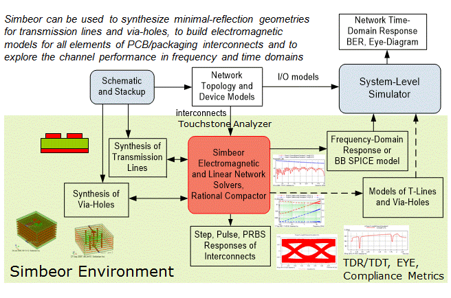
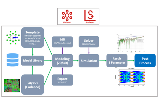
    SIMBEOR is a 3D electromagnetic signal integrity tool for simulating and analyzing the entire interconnect link. It offers an industry-first measurement-validated electromagnetic signal integrity software for the physical design of PCB and packaging interconnects for communication links operating at 6-112 Gb/s and beyond. Simbeor is the one-stop solution for all interconnect budget exploration (advanced stackup planning and pre-layout), design verification (post-layout), dielectric and conductor roughness models identification, and macro-modeling tasks. The accuracy of the models is ensured by the use of advanced algorithms for 3D full-wave analysis, benchmarking, and experimental validation. It fits any design flow as a system interconnect budget exploration tool, interconnect verification tool, or a Touchstone model clean-up and macro-modeling tool for automatic S parameter extraction.

    Simbeor Solvers and Algorithms:

    Simbeor 3DML™ : Full-wave 3D analysis tool for multi-layered geometries:

    • Hybrid solver : Method of Lines + Trefftz Finite Elements + Method of Simultaneous Diagonalization (de-embedding)
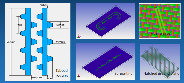
    • Analysis of discontinuities and transmission lines with high-frequency (non-TEM) dispersion and anisotropy (any planar cross-section)
    • Simbeor 3DTF™ : First full-wave 3D analysis tool based on Trefftz Finite Elements (aka Ultra-Weak Discontinuous Galerkin's Wave Elements)

    Simbeor SFS™ : Unique quasi-static field solver for large t-line cross-sections (any planar cross-section):

    • MoM : Supports all dispersive isotropic material and conductor roughness models
    • Linear Network solvers : Unique port-based circuit analysis with 7 solvers for frequency and time domain analyses of multiport networks based on Y or S-parameters (with sparse solvers for extremely large multiport networks), capabilities to extract GMS-parameters, test fixture S-parameters and de-embed test fixture
    • Rational Compactor™ : Converts discrete S-parameter models into frequency-continuous rational macro-models for consistent frequency and time domain analyses

    Simbeor : Tools and Interfaces:
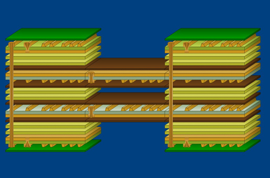
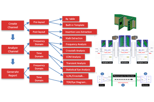
    Board Analyzer™ : Post-layout decompositional electromagnetic analysis
    Transmission Line Wizard - Fast synthesis of any single-ended and differential line geometries (strip, microstrip, CPW, CBCPW)
    Via Analyzer™ : Fast synthesis of via-holes and launches geometry
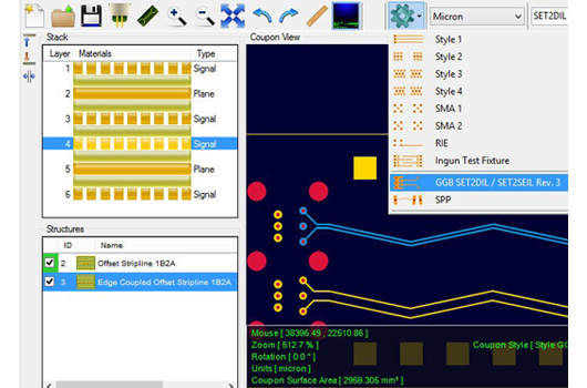
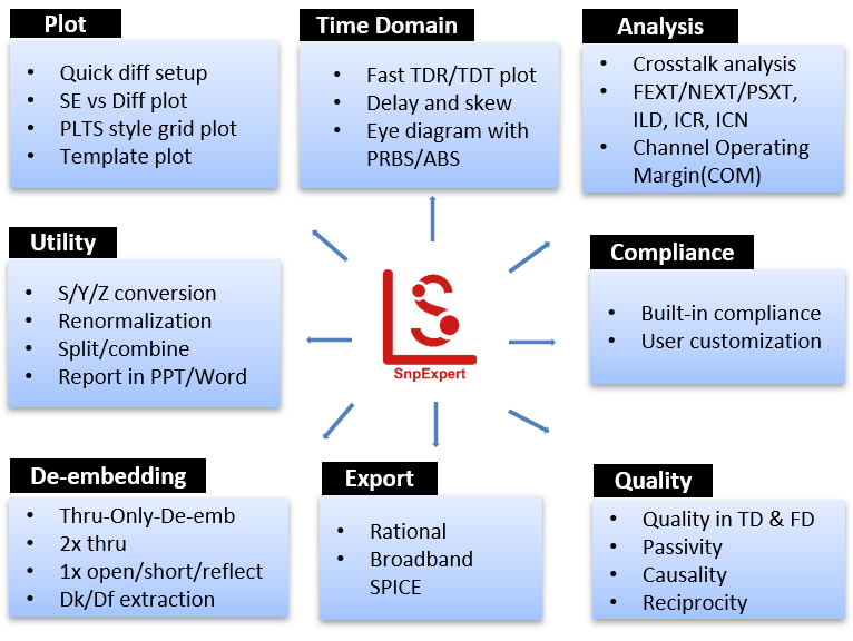
    Touchstone Analyzer™ : S-parameters plotting, quality assurance, and rational macro-modeling
    Geometry Editor : Pre and Post-layout analyses of multi-layered circuits
    Linear Network Editor : Draw or edit multiport networks (link path models)
    SiTune™ : Material models, geometry and linear network optimization
    Board Geometry Translators : ODB++, HyperLynx hyp-file, Allegro brd/mcm, PADS ASCII
    Violation Browser™ : Violation viewer for EMSAT rule checker
    Eye Analyzer™ : Computation of eye diagram metrics and comparison of eye diagrams
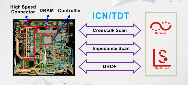
    ICN Analyzer™ : Computation of Integrated Crosstalk Noise and a quick comparison with compliance mask
    Interactive Graphs : Plot transmission line modal and RLGC(f) parameters, S-parameters, 10G and 25G compliance metrics, TDR/TDT, eye diagram
    Batch Mode - Run analysis in batch mode for design automation
     

    Download SIMBEOR Brochure

    Applicable only in Greater China, India, Vietnam, Malaysia, Thailand, and Singapore.

    Xpeedic: ChannelExpert – Channel Exploration

    ChannelExpert provides a fast, accurate and easy way to evaluate and analyze pre-layout or post-layout high speed channel with its built-in advanced circuit and EM solver technologies.

    It is challenging for digital system designers to simulate a high-speed SERDES channels. There are many different simulation scenarios to cover ranging from pre-layout / post-layout, frequency-domain / time-domain / statistical analysis, compliance check, to TX / RX optimization. 

    ChannelExpert offers many built-in channel templates to support pre-layout exploration. Parametric S-parameters and transmission line models are supported for easy channel exploration. For post-layout scenario, ChannelExpert can extract the desired channels with or without crosstalk from physical layout with transmission line and 3D via models automatically generated with inbuilt field solvers.

    Key Features

    • Built-in 2D RLGC solver to model TML
    • Easy multiple channel creation by table with only one-click
    • Built-in template to quickly create single channel and multiple channel
    • Easy to import PCB file to create channel
    • Support full BP simulation for Traditional BP, Orthogonal Direct BP, Orthogonal Mid-Plane BP
    • Support generating high speed SERDES channels from a bunch of PCB files and perform crosstalk and insertion loss simulations
    • Support buffers with DFE, CTLE and FFE, automatically optimize the equalization coefficient based on channel characteristics
    • Built-in substrate and stackup databases to modeling TML
    • Parametric S-Parameter files and transmission line physical parameters for easy channel exploration
    • Add multiple interpolation and extrapolation algorithms for S-parameter based frequency domain and crosstalk analysis
    • Support COM (Channel operation margin) analysis
    • Seamlessly link to SnpExpert for S-parameter viewing and post-processing

    Download ChannelExpert Brochure

    Xpeedic: ViaExpert – Via Modeling and Simulation

    ViaExpert provides a fast and accurate way to model and simulate vias. It allows designers at the pre-layout stage to quickly build via models and check the key signal integrity metrics such as insertion loss, return loss, and crosstalk. It also allows designer to perform post-layout simulation of vias and trace breakout.

    To quickly build via models, ViaExpert provides multiple ways including built-in templates, direct layout file import and a combined flow which takes advantage of both the layout trace breakout and built-in templates. ViaExpert deploys two field solver technologies, Finite Element Method (FEM) solver, and the another a hybrid field solver. Both adopt distributed processing and multi-core parallelization, which adds another level of acceleration to model computation.

    Key Features

    • Optimization mesh improves the simulation accuracy and speed
    • Fast 3D FEM and hybrid solver offers better capacity and speed compared to other tools in market
    • Support HPC, remote and local simulation under the management of XDPM (Xpeedic Distributed Processing Management) module to maximize high computing machine availability
    • Built-in connector footprint library, easy to build connector via model
    • Multiple ways to create Via models or import Cadence .brd, .mcm, .sip file
    • Support arbitrary Via array definition, move, duplicate, align top / bottom / left / right, distribute horizontally / vertically, undo and redo features in 2D footprint window
    • Easy to add Via tear drop and trace compensation
    • Easy to modify stackup, trace length, trace width, pad size and antipad size
    • Support arbitrary parameterized keepout definition, management and usage in 2D footprint window to explore the optimal antipad geometry, the keepout shape can be defined by the unite of lines / arcs or regular parameterized geometries
    • Optimize routing method and support to define trace by axis or segment
    • Auto port generation, simplifies EM analysis setup
    • 3D-View makes the model check easier
    • Support parametric and optimization sweep simulation
    • Support export models to third-party tools, such as HFSS or CST

    Download ViaExpert Brochure

    Xpeedic: SnpExpert – S Parameter Exploration

    Xpeedic SnpExpert provides a quick way to understand the electrical characteristics of passive interconnectors in a system by viewing the S-parameter in frequency domain and examining the time domain reflectometry (TDR). One-click definition of differential pairs and victim / aggressor setup, together with the built-in NEXT, FEXT, PSXT, ILD, ICR, and ICN, allows user to quickly evaluate the crosstalk.

    Key Features

    • One-click to define differential pairs and victim / aggressor pairs
    • Built-in compliance metrics, such as IEEE802.3, OIF CEI etc.
    • Built-in template plot for RF components
    • Built-in Thru-Only De-embedding (TOD)
    • Built-in Open-Short / Thru De-embedding (OTD) method for on-chip de-embedding
    • Built-in delay & skew calculator
    • Support multiple data curves gating with only one click and export S-parameter
    • Built-in RLGC solver for transmission lines
    • Multi-ways to extract Dk / Df from S-parameter file
    • Built-in passivity / causality / reciprocity / stability checker
    • Support to convert S-parameter to broad band spice or Hspice RFM model
    • Support S->RLGC, RLGC->S, S->W-element transformation
    • Support complex numbers for S-parameter
    • Support to combine multiple s4p files to one snp
    • Support for Touchstone 2.0
    • Support Python script to invoke most SnpExpert features, including S-parameter import, plot, add mark, TDR, TOD and so on
    • Easy to generate report in MS Word and PPT format

    Download SnpExpert Brochure

    Xpeedic: TmlExpert – Fast and Accurate TML Modeling and Simulation

    TmlExpert is an application which is used to deal with TML modeling and simulation. It provides a fast and convenient method to create TML model, from simulation result check, such as insertion loss, return loss, crosstalk, also allows the designer to do the simulation and tracking processing for the post layout.

    TmlExpert has three solver technologies including 2D RLGC, 2.5D MoM and 3D FEM to achieve the best accuracy and convenience and has various templates for transmission-line structures including hatched ground plane and fiber weave

    Key Features

    • Fast FEM3D and 2D RLGC solver offers better capacity and speed
    • Optimal 3D mesh improves the simulation accuracy and speed
    • Support adaptive frequency sweep and multi-threading processing technology to achieve excellent performance speedup
    • Built-in multiple templates for easy transmission line electrical characteristic exploration, including Tabbed Routing template, Serpentine Routing template and traditional Transmission Line template
    • Auto port generation simplifies EM analysis setup
    • 3D-View makes the model check easier
    • Support export models to third-party tools, such as HFSS

    Download TmlExpert Brochure

    Xpeedic: CableExpert – Fast and Accurate Cable Modeling and Simulation

    Cable assembly is a key building component in network systems. Accurate modeling of cables is becoming a necessity to achieve the desired signal integrity with multi-gigabit data rate. Twin axial cable used for SFP and QSFP interface in 10G / 40G / 100G Ethernet is such an example. Many parameters have significant impact on signal quality such as drain type and shielding pattern, to name a few. Engineers need a fast and accurate way to model and simulate the cable with high confidence in signal integrity.

    CableExpert offers a quick way to build 3D models with its built-in templates

    • Various drain types including center drain and dual drain
    • Various twin shielding including longitudinal and wrapping
    • Auto port generation to simplify EM setup
    • Parametric sweep for easy what-if analysis

    Key Features

    • Fast 2D FEM RLGC solver offers better capacity and speed compared to other tools in market for cable simulation
    • Support adaptive frequency sweep and multi-threading processing technology to achieve excellent performance speedup
    • Optimal 2D mesh improves the simulation accuracy and speed
    • Auto port generation simplifies EM analysis setup
    • Support parametric and optimization sweep simulation for Twin axial Cable, Twisted Cable, LVDS Cable, IEEE 1394, Differential Cable and USB type-C templates
    • Easy export CableExpert simulation project to HFSS for easy verification

    Download CableExpert Brochure

    Xpeedic: Heracles - Automated SI Signoff for High Speed Design

    Heracles is the first SI signoff tool for high speed designs. It integrates a novel hybrid full-wave EM solver with the same accuracy order as the conventional 3D solver but at a much higher speed. The hybrid solver takes advantage of the layered nature of the PCB layout and adopts the idea of layer-by-layer decomposition to reduce the complexity of the problem and achieve the computation speed optimized for full board crosstalk scan. With automated SI signoff flow, we can achieve the complete full board crosstalk scan in a few hours as intended with using the tool, which significantly reduces the post-layout check time, allows layout optimization, and ensures the full board coverage.

    Heracles enables SI engineers to scan the Via pin field and breakout region under connectors or BGA packages for impedance and crosstalk violation. Crosstalk metrics such as frequency domain integrated crosstalk noise (ICN) or time domain waveform TDT are derived from the S-parameter to quantify crosstalk.

    Key Features

    • Built-in versatile EM solver engines with controllable accuracy and speed to achieve full board scan within a few hours, including FEM3D solver, Hybrid Solver and Pure Via Solver
    • Built-in high speed I/O compliance such as Ethernet, PCI Express, DDR, USB, SATA and SAS, where crosstalk poses great challenges for high speed PCB designers with the ever-increasing data rate
    • Provides two flexible ways to select crosstalk scan areas with potential SI issues, either by net matching rules defined in high speed I/O compliances or selected manually
    • Heracles XSE provides interactive interface to invoke ViaExpert to visualize, sweep and optimize crosstalk model, and export to HFSS for better correlation

    Download Heracles Brochure