Test


Polar UK: Atlas Si VNA PCB Insertion Loss measurement system

Atlas for Anritsu VNA is compliant with IPC TM650 2.5.5.12 (Test Methods to determine the Amount of Signal Loss on Printed Boards) and provides support for Delta-L methodology.

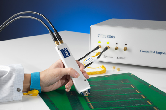
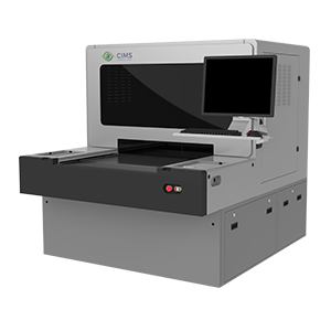
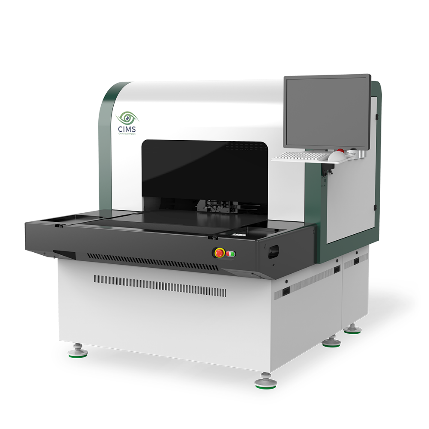
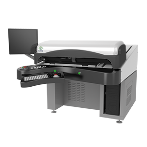
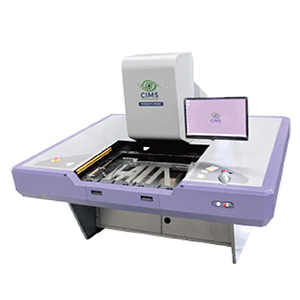
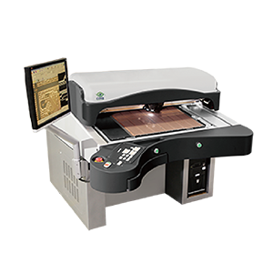
Atlas Si is a high precision insertion loss measurement package designed specifically for PCB fabricators and OEMs. It provides accurate, repeatable measurements of frequency-based transmission line losses, allowing fabricators to meet stringent targets that maintain signal integrity within the limits of the latest high-speed chipsets.

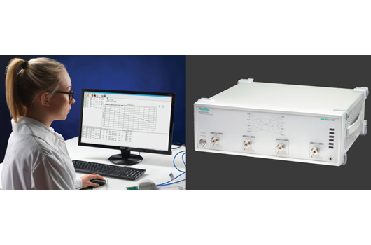
Polar has partnered Anritsu for integrating their Anritsu ShockLine™ 4-Port Performance VNA (vector network analyzers) with Atlas. Anritsu ShockLine™ 4-Port Performance VNAs achieve a new level of capability, flexibility, and value for RF and microwave network analysis applications delivering excellent performance for measurements from 50 kHz up to 43.5 GHz. These instruments are ideal for testing passive and many active components with general purpose VNA requirements. The ShockLine family employs advanced Anritsu technology and design expertise to attain outstanding dynamic range, calibration and measurement stability, and speed performance in efficiently packaged, compact, and robust VNA instruments.

Anritsu ShockLine™ 4-Port Performance VNA Key Features and Benefits

  • Time domain with time gating option enables easier and faster fault identification in broadband devices
  • Patented non-linear transmission line (NLTL) technology delivers wider bandwidth and higher dynamic range than competing technologies, enabling better measurement accuracy and repeatability with longer intervals between calibrations
  • Multiple calibration methods to choose from to best suit your application – SOLT, SOLR, SSLT, SSST, LRL, LRM, or Thru update
  • Precision AutoCal™ or SmartCal™ for an easy, one-button automatic method of VNA calibration
  • Eliminates the need for over-specified, high-end VNAs with extra features not required for production testing
  • Anritsu’s Extended-KTM connectors enable ShockLine frequency option 43 VNAs to offer guaranteed performance to 43.5 GHz in a K/2.92 mm compatible form factor

Download Brochure

Note: Anritsu Corp., USA are the sole owners of following trade marks for ShockLine™, AutoCal™, SmartCal™ and Extended-KTM

Polar UK: CITS880s - Controlled Impedance Test System

CITS880s system is the 9th generation impedance test system from Polar Instruments Ltd, UK. It is a solution for fabricators who need to measure impedance on fine traces and thin copper. CITS880s features Launch Point Extrapolation (LPE) that extrapolates the TDR response to a point close to the start of the transmission line effectively aloowing users to measure the instantaneous or incident impedance of the line more acccurately.

In addition to the LPE the CITS880s is also capable of measuring shorter traces - typically 2-3 inches shorter than previous generation of the CITS series. CITS880s now ships with completely re-engineered IPS and IPDS high speed probes whcih reassuringly are precision moulded with ESD dissipative materials to give maximum protection to your CITS.

Polar IPS and IPDS high speed probes are specifically desgined for CITS880s. They combine revised internals with more robust mechanical design and enhancements to the signal path, along with ergonomic precision mouldings in 100% ESD dissipative materials. IPS and IPDS probes are easily identified and contrast with previous generation probes by the use of the blue labels and blue resists on the probe tip interface.

Click here to see what's new in the CITS880s.

Polar GmbH: RITS550/RITS880 – Automated Impedance Measurement System

RITS 550 automates the industry standard CITS880s (Controlled Impedance Test System) to give fast, repeatable volume testing of coupons and PCBs. The system is controlled via easy to use Windows software. Test set-up is straight forward, results data is automatically logged in accessible formats, and there is the option of a built-in report generator.

Accurate, traceable measurement RITS550 uses proven time domain reflectometry (TDR) techniques to measure the reflection of fast rise-time pulses. High precision reference airlines - traceable to NPL and NIST standards - ensure repeatable measurement accuracy to allow the trace impedances to be controlled.

With test times as fast as fixture-based systems, RITS550 flying probe technology provides unparalleled levels of measurement repeatability, with a lifetime cost of ownership that is just a fraction of a fixture-based system.

RITS880 is a built to order automated impedance measurement system which is larger version of the RITS550. It can incorporate full sized panels and can be equipped with an automatic loader/unloader to provide full automation for impedance testing.

Click here to download brochure for RITS550

Click here to download brochure for RITS880

PWB: IST HC- Interconnect Stress Test System

Interconnect Stress Test or IST is an accelerated stress test method developed by PWB Interconnect Solutions Inc., Canada that overcomes the limitations of thermal oven or liquid / liquid test methods. It has the capability of effectively and rapidly quantifying the integrity of different types of vias including microvias. IST creates a uniform strain from within the substrate and the interconnects ability to distribute and redistribute this strain provides an indication of integrity. The plated barrels and inner layer junctions are “exercised” until the initial failure mode / mechanism is uncovered.

The IST HC uses IST technology to electrically cycle test coupons to determine the reliability of a product. In addition to supporting IPC Test Method 2.6.26, the latest IST HC now supports IPC Test Method 2.6.27 to simulate Lead Free Solder assembly. The IST HC can simulate both the reflow oven and assembly rework station temperature profiles to subject the test coupon to the same temperature excursions as experienced by actual printed circuit board during assembly process.

IST has become the leading test standard for via and material reliability. Top OEMs, ODMs, CDMs, PCB material and PCB manufacturers around the world use IST technology to test new via / interconnect technologies, materials and processes.

The test system incorporates custom designed power supply and high precision measurement systems which are interfaced to a user-friendly application software, that automatically measures, records, analyzes data with displays and reports that simplify the understanding of the reliability of a custom designed test vehicle / coupon that represents the actual product.

Download Brochure

Download IPC-TM-650 Test Method

CAF (Conductive Anodic Filament) tester
CAF is a fully automated bench top CAF measurement equipment with RH control, temperature control, V Bias control, custom profiles and remote reporting.

Download Brochure

DELAM - Dielectric Estimation and Laminate Analysis Measurement System
DELAM automatically measures and analyzes changes in material properties that signify whether damage was caused by exposure to the elevated temperatures associated with component assembly and possible reworks

Download Brochure

CIMS HK: Automated Optical Inspection Systems (AOI)

Automated optical inspection (AOI) is a crucial step for PCB manufacturers, during which inner and outer layers are carefully inspected to assure functionality and reliability resulting in high yield production. 

CIMS offers wide range of AOI systems for all segments of PCB industry – from IC Substrates and HDI, flex and rigid flex to mainstream multi-layer boards. CIMS AOIs are helping our customers to dramatically increase yield of PCB manufacturing process as well as improve quality of the final product. Various models available are: 


Galaxy 4Cχ 

Galaxy 4Cχ, equipped with color camera, is designed to support high volume manufacturing of next generation IC Substrates. It is capable to scan down to 4 µm line/space width technology. 


Galaxy 5Cχ 

Galaxy 5Cχ, equipped with color camera, is designed to support high volume manufacturing of highly advanced IC Substrates. It is capable to scan down to 5 µm line/space width technology. 


Galaxy 7Cχ 

Galaxy 7Cχ, equipped with color camera, is designed to support high volume manufacturing of advanced IC Substrates. It is capable to scan down to 7 µm line/space width technology. 


Galaxy 10Cχ 

Galaxy 10Cχ, equipped with color camera, is designed to support high volume manufacturing of advanced IC Substrates and ultra fine line HDI. It is capable to scan down to 10 µm line/space width technology. 

CIMS HK: Automated Optical / Final / Verification (AOI / AFI / AVI) Inspection Systems (Only in India)

CIMS AOI, AFI and AVI systems combined with 2D and 3D metrology tools are capable to scan lines of down to 4 µm and are widely used in all segments of PCB industry.

CIMS HK: AI-Powered Hybrid Verification Systems


AIVR 4μ 

AIVR, CIMS AI-powered verification station that combines virtual and physical verification within a single workstation. AIVR 4μ is designed to support high volume manufacturing of IC Substrates and optimized for verification of 4 ~ 15 µm line/space width technology. 


AIVR 5μ 

AIVR, CIMS AI-powered verification station that combines virtual and physical verification within a single workstation. AIVR 5μ is designed to support high volume manufacturing of IC Substrates and optimized for verification of 5 ~ 25 µm line/space width technology. 


AIVR 7μ 

AIVR, CIMS AI-powered verification station that combines virtual and physical verification within a single workstation. AIVR 7μ is designed to support high volume manufacturing of IC Substrates and optimized for verification of 7 ~ 25 µm line/space width technology. 


AIVR 10μ 

AIVR, CIMS AI-powered verification station that combines virtual and physical verification within a single workstation. AIVR 10μ is designed to support high volume manufacturing of HDI and IC Substrates and optimized for verification of 10 ~ 25 µm line/space width technology. 


CIMS HK: Photo Tools Inspection Systems


Phoenix PT/Micro 

Phoenix PT/Micro, CIMS photo-tools AOI system, is designed to inspect high-resolution film artworks and glass masks. It is capable to scan down to 7 µm line/space width technology. 


Phoenix PT+ 

Phoenix PT+, CIMS photo-tools AOI system, is designed to inspect high-resolution film artworks and glass masks. It is capable to scan down to 12.5 µm line/space width technology. 


CIMS HK: Hybrid Verification Systems

VVR for ICS 

VVR, CIMS hybrid-mode verification station that combines virtual and physical verification within a single workstation. VVR for ICS is designed to support high volume manufacturing of IC Substrates and optimized for verification of 4 ~ 15 µm line/space width technology.